



Sorry, no sales person is available right now to take your call. Pls leave a message and we will reply to you via email as soon as possible.
Home/ PCB News/ A Comprehensive Guide to Memory PCB Design: Key Points for SRAM, DDR, and Flash
A Comprehensive Guide to Memory PCB Design: Key Points for SRAM, DDR, and Flash
2026-03-30
This PCB Layout Memory Design Guide is extremely technical, directly addressing the three core aspects of stability, speed, and yield. BaiNeng YunBan has organized it into a clearer version that you can directly bookmark and use for PCB fabrication verification—more compact in structure and with more prominent key points, enabling engineers to apply it immediately.
PCB Layout: Core Guidelines for Memory Design
(Comprehensive Summary for SRAM / DDR1~5 / EEPROM / Flash)
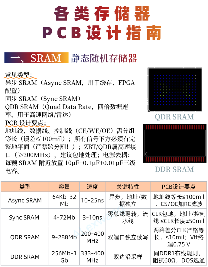
1. SRAM — Fast but Sensitive to Interference
Types: Asynchronous SRAM (ZBT), Synchronous SRAM, QDR SRAM (used in high-speed networking / radar)
Layout Guidelines:Group address, data, and control signals with matched lengths
CE/WE/OE, address, and data grouped with length mismatch ≤100 mil
Solid ground plane—no split crossings allowed:All signals must have continuous GND underneath
Ground shielding recommended for high-speed SRAM:For ZBT/QDR ≥200 MHz, add ground traces on both sides of signals to reduce crosstalk
Three-level decoupling:Place capacitors close to each chip: 10μF + 0.1μF + 0.01μF
Typical Risks:Unequal trace lengths → sampling window shift → read/write failures or system crashes
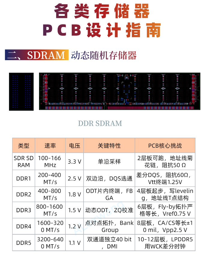
2. DRAM (DDR1~DDR5) — Most Stringent Timing Requirements at High Speed
Universal Golden Rules (Applicable to DDR3~DDR5)
Command / Address / Control: Fly‑by Topology
CLK/CKE/CS/RAS/CAS in daisy-chain; T-branching strictly prohibited
DDR3 requires VTT termination resistors; DDR4/DDR5 use ODT (On-Die Termination)
DQ/DQS: Strict Point-to-Point Routing
One DQS pair serves 8/16-bit DQ; no branching allowed
Intra-group length matching requirements:
DDR3: ≤50 mil
DDR4: ≤20 mil
DDR5: ≤10 mil
Differential Clock CLK±
100Ω differential impedance
Length mismatch ≤10 mil
Keep away from DQ lines and power traces; spacing ≥20 mil
Clean Power Domain Partitioning
Strict separation of VDD / VDDQ / VREF planes
Dense placement of 0402 decoupling capacitors near memory pins
VREF should be supplied by a dedicated low-noise LDO
Reference Plane Requirements
Signal layers must be adjacent to a solid GND plane
No split crossings or high-frequency/high-current traces beneath DDR area
Typical Risks
Un-terminated Fly‑by → severe signal reflections
DQ length mismatch → closed eye diagram, read/write errors
VREF noise → dramatically increased BER, inability to achieve rated frequency
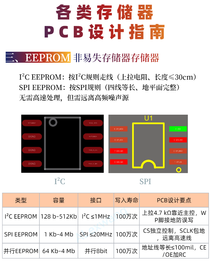
3. EEPROM — Low Speed but Demands Reliability
I²C EEPROM
Follow I²C specifications; add appropriate pull-up resistors on SDA/SCL
Trace length generally ≤30 cm
Keep away from clock and power supply noise
SPI EEPROM
Keep CS/CLK/DIO/DO traces as length-matched as possible
Maintain solid ground plane underneath
Impedance control not required, but avoid proximity to noise sources
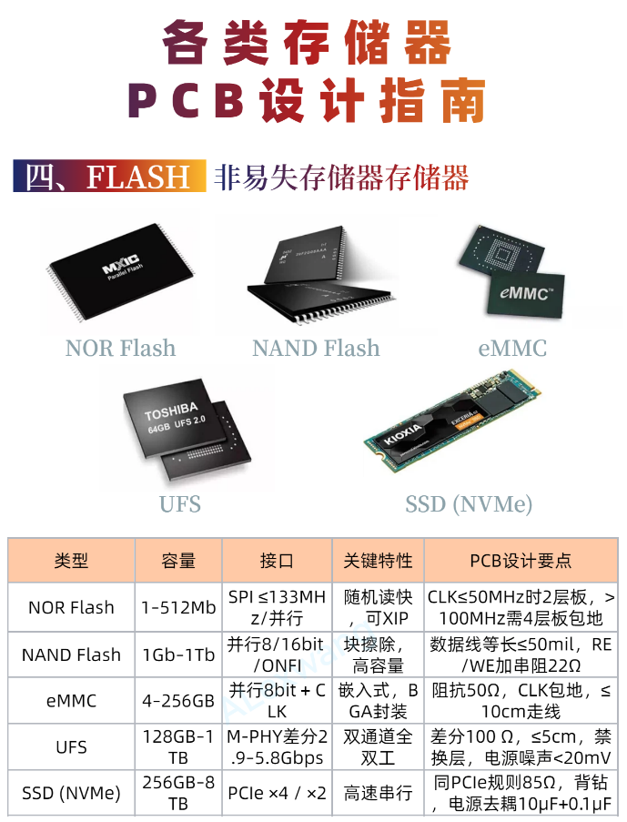
4. Flash Types — Parallel vs. High-Speed Interfaces Differ Significantly
1. NOR Flash
Parallel NOR
Address / Data / Control grouped with length mismatch ≤100 mil
OE/WE/CE routed synchronously
Solid ground plane required
Serial NOR (SPI / QSPI)
QSPI IO0~3 length mismatch ≤50 mil
Clock (CLK) trace should be ground-shielded
For frequencies >50 MHz, impedance control is recommended
Risks
Unequal trace lengths in parallel Flash → address corruption, failed ID reads
2. NAND Flash
Parallel NAND
Timing more sensitive than NOR; stricter length matching required
ONFI / Toggle DDR NAND
Uses differential DQS similar to DDR architecture
DQ + DQS intra-group length mismatch ≤20 mil
Continuous ground reference throughout; no split crossings allowed
3. eMMC / UFS
eMMC (HS200 / HS400)
8-bit data + clock length mismatch ≤50 mil
Clock (CLK) trace should be ground-shielded; keep away from RF and switching power supplies
UFS
High-speed MIPI differential pairs with 100Ω impedance
Layout standards similar to MIPI CSI/DSI
Risks
eMMC length mismatch → downgrades from HS200 to HS52, significantly reduced speed
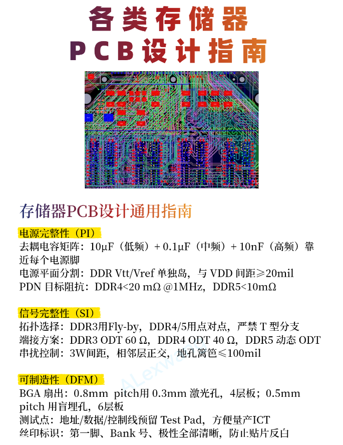
SRAM: Group length matching ≤100 mil + solid ground + three-level decoupling
DDR: Fly‑by command/address + strict DQ/DQS length matching + differential clock + clean power partitioning + no split crossings
EEPROM: I²C pull-ups / SPI length matching + noise isolation
NOR Flash: Parallel length matching; QSPI length matching + ground shielding
NAND/eMMC: DDR-like timing; DQS/data length matching; solid ground reference
trending news
Contact Us