



Sorry, no sales person is available right now to take your call. Pls leave a message and we will reply to you via email as soon as possible.
Home/ PCB News/ PCB Backdrilling Process: Technical Essentials, Application Scenarios, and Design Guidelines
PCB Backdrilling Process: Technical Essentials, Application Scenarios, and Design Guidelines
2026-01-26
1. Process Definition and Core Value
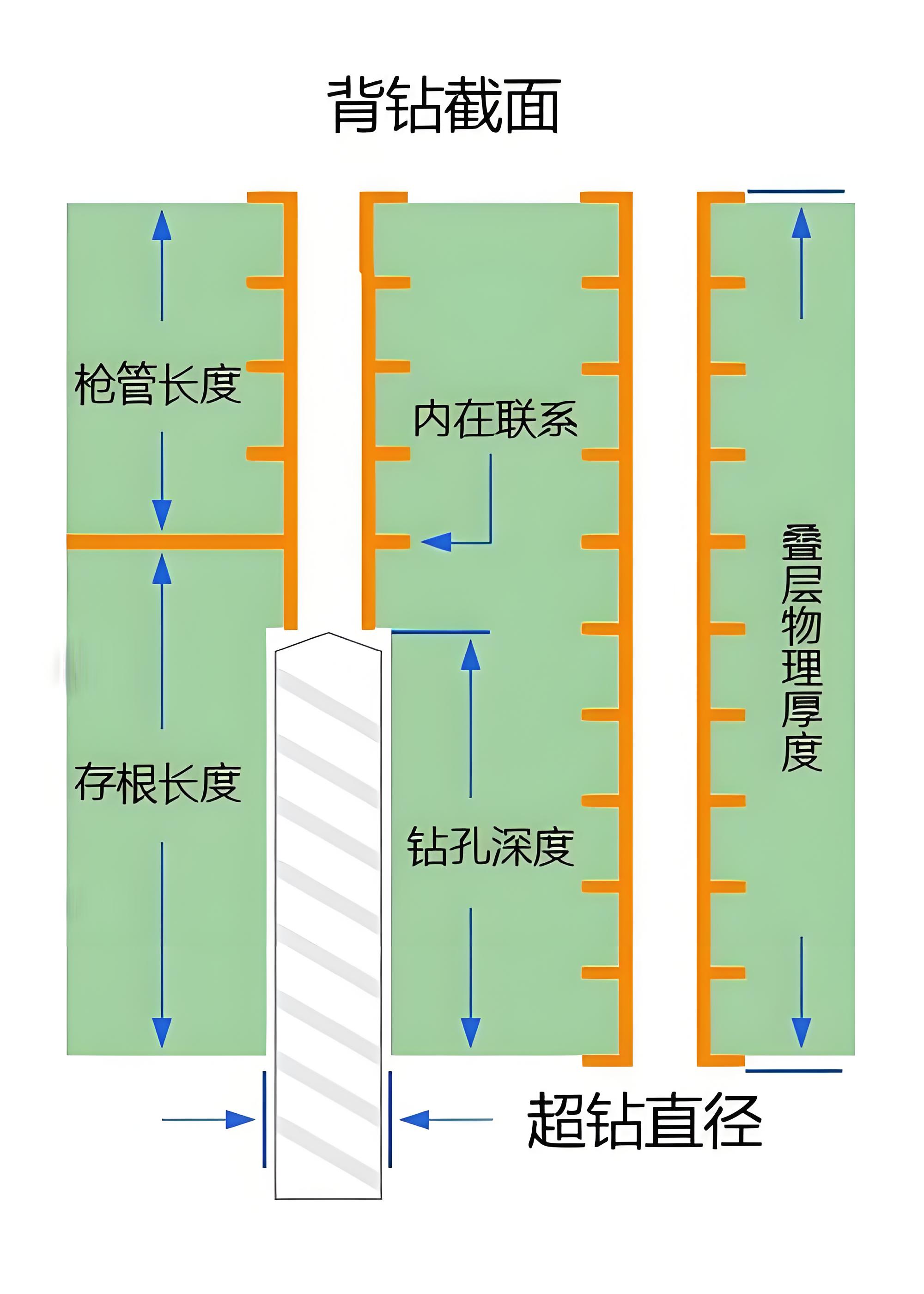
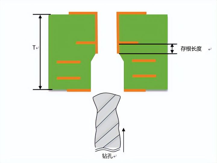
Back drilling is a high-precision specialized process in PCB manufacturing. Its essence lies in precisely controlled depth drilling to remove unnecessary copper stubs from vias. The core value of back drilling is to address signal reflection, loss, and interference issues in high-speed/high-frequency signal transmission, ensuring signal integrity (SI) and system stability. It is one of the key processes enabling high-performance interconnects in advanced PCB products.
2. Core Application Scenarios and Design Requirements
Application Domain | Typical Scenarios/Products | Core Signal Characteristics | Key Back Drilling Requirements and Objectives |
|---|---|---|---|
High-Speed Digital Communication | Routers, Switches AI Servers, Data Center Equipment | Multi-Gigabit-per-second (Gbps) High-Speed Differential Signals Rates Often Reach 10 Gbps or Higher | Shorten stub length to suppress signal reflection and jitter Ensure eye diagram quality meets specifications and satisfy reliability requirements for high-speed data transmission |
High-Frequency RF/Wireless | Base Station Antennas, Power Amplifiers (PA) Radar, RF Modules | High-Frequency Analog Signals Frequencies Often Range from Several GHz to Dozens of GHz | Reduce parasitic capacitance and inductance introduced by stubs, suppressing resonance effects Minimize signal distortion and insertion loss |
High-Speed Computing and Storage | CPU/GPU Motherboards, Memory Modules (DDR5/DDR6) AI Accelerator Cards | Extremely High Data Rates Stringent Timing Control and Impedance Matching Requirements | Optimize via impedance continuity, reducing deterministic jitter (DJ) and random jitter (RJ) Enhance system computing and storage stability |
Other Specific Scenarios | Optical Module PCBs Specialty Interconnect Boards | Special Interconnect Requirements Some Involve High-Speed Signal Transmission | Drill through temporary conductive leads to meet special structural interconnect requirements Assist in optimizing overall signal transmission performance |
3. Criteria for Determining the Necessity of Back Drilling
The decision to implement back drilling primarily depends on the impact of signal speed and stub electrical length on signal integrity. The core evaluation criteria are as follows:
1. Core Quantitative Criterion
Back drilling must be employed when the electrical length of the via stub exceeds 1/10 of the signal’s rise-time equivalent electrical length. In engineering practice, this quantitative criterion typically corresponds to scenarios with signal rates ≥1 Gbps—meaning that when signal rates reach or exceed 1 Gbps, stub impact must be carefully evaluated and back drilling planned accordingly.
2. Authoritative Validation Method
The most reliable approach is to perform system interconnect channel simulation (using tools such as Ansys or Cadence). By modeling and analyzing the specific effects of stub length and impedance characteristics on signal reflection, loss, and jitter, engineers can accurately determine whether back drilling is needed and define the required drilling depth.
4. Core Process Flow and Technical Considerations
1. Standard Process Flow
Back drilling must be integrated with standard PCB manufacturing steps. The core sequence is: Primary Drilling → Via Metallization (PTH and Plating) → Back Drilling from Opposite Side (to a safe position above the target layer) → Cleaning (removal of drill debris) → Quality Inspection
2. Key Technical Considerations
Precise Depth Control: Achieved using high-precision CNC drilling machines (e.g., Schmoll from Germany or Hitachi from Japan), employing closed-loop Z-axis control, optical alignment calibration, and real-time board thickness compensation to enable micron-level depth accuracy. To avoid damaging the target layer pad, a safety margin of 8–10 mil (approximately 0.2–0.25 mm) is typically maintained above the target pad, with depth tolerance requirements of ±5–10 mil.
Drill Bit Sizing: The back drill bit diameter should be 8–10 mil (0.2–0.25 mm) larger than the original via diameter to fully cover and remove the copper stub on the via wall, preventing residual conductive material from degrading signal performance.
Process Integration Optimization: Back drilling is often followed by resin plugging, where high-temperature-resistant, low-CTE specialty resin fills the drilled cavity to prevent contamination in subsequent processes and maintain surface planarity for lamination, solder mask application, and other steps.
Quality Inspection Techniques: Traditional methods use metallographic cross-sectioning (destructive testing), which visually reveals stub length but is inefficient. Advanced solutions (e.g., BAINENG Yunban’s patented technique) employ dedicated test vias and circuits, enabling rapid, non-destructive verification of stub length compliance via continuity or impedance testing—improving inspection efficiency by over 80%.
3. Design-Manufacturing Collaboration Essentials
Back drilling increases PCB manufacturing cost (by approximately 10–20%) and lead time (by 1–2 working days). Close collaboration with the manufacturer during early design stages is essential, with key considerations including:
Clear Specification Documentation: Explicitly annotate networks requiring back drilling, target layers (start and stop), desired residual stub length (recommended ≤8 mil), and tolerance ranges in Gerber files and manufacturing specifications.
Manufacturing Capability Verification: Confirm the PCB fabricator’s back drilling capabilities in advance, including depth control tolerance (standard ±5–10 mil; high-end can achieve ±3 mil), minimum annular ring guarantee (recommended ≥8 mil), and compatibility with resin plugging.
Design-Level Optimization: Minimize the number of unused layers penetrated by high-speed signal vias to inherently reduce stub length; avoid placing back drill holes in densely packed pad areas to lower alignment difficulty and risk of damage.
5. Future Development Trends
As AI, 5G, and high-speed computing continue to raise PCB performance demands, back drilling technology is evolving toward “ultra-high precision, intelligence, and multi-technology integration,” with key trends as follows:
Extreme Precision Enhancement: New technologies like 3D inner-layer conductive single-pass back drilling and thickness-memory compensation can improve stub length control by over 40%. In high-end applications, stub lengths can be maintained below 5 mil to support ultra-high-speed signaling (e.g., 56 Gbps and beyond).
Intelligent and Automated Upgrades: CAM software integrated with AI algorithms can automatically identify high-speed nets, select vias requiring back drilling, and optimize drilling paths. Combined with CCD vision alignment and laser distance measurement, back drilling alignment accuracy now reaches the micron level, significantly reducing human error.
Multi-Technology Convergence: In advanced HDI (High-Density Interconnect) and any-layer interconnect boards, back drilling is deeply complementary to blind vias, buried vias, and laser microvias. Hybrid approaches such as “blind/buried vias + back drilling” enable compact, high-density, high-performance PCB designs.
trending news
Contact Us